Achievement Award
Pioneering research on silicon integrated photonic circuits


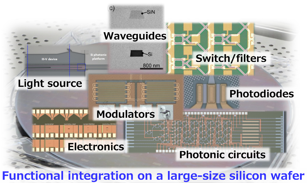
Silicon photonics is an integrated photonic circuit technology based on a silicon electronics fabrication technology. The basic concept of this technology is illustrated in Fig. 1. Silicon photonics enables the functional integration of various photonic circuits, and moreover, enables significant reductions of circuit size, energy consumption and fabrication cost. Furthermore, it can integrate electronics circuits with photonics ones. Therefore, silicon photonics has recently been applied to high-speed large-capacity data transmission in data centers and distributed computing systems. Other wide-range applications, such as sensor devices for consumer health care, are also expected in the near future.
The recipients, Drs. Yamada, Tsuchizawa, and Fukuda, started research on silicon photonics around 2000. In this early stage of the research, neither the issues nor the potential applications of integrated photonic circuits had yet been shown because building photonics with CMOS fabrication processes was too ambitious. To explore such an uncharted technical field, they first started developing a low loss silicon waveguide system, and soon demonstrated a very low loss fiber-waveguide coupling structure, in which the coupling efficiency was over 90% [1,2]. The schematic structure of the fiber-waveguide coupling is shown in Fig. 2(a). This work had a great impact on the field of silicon photonics. Their developed fiber-waveguide coupling structure and its variations have been used widely in silicon photonic circuits around the world. Thereafter, they developed low-loss silicon waveguides and various waveguide-based elemental devices, such as ultra-compact add/drop filters [2,3]. The structure of the original add/drop filter is shown in Fig. 2(b). Thus, they became among the first to demonstrate the potential of silicon photonics as a platform for integrated photonic circuits [2]. They have also developed a very important technique realizing polarization diversity circuits [4]. The schematic structure of such circuits is shown in Fig. 2(c). Since polarization dependence is one of the intrinsic deficiencies of silicon photonics, this work also had a significant impact on silicon photonics. Indeed, their proposed polarization diversity technique has become a world-standard method of building polarization independent circuits. While developing the photonic devices shown above, they focused on the significant enhancement of optical nonlinear effects in silicon waveguides, and demonstrated a high-efficiency wavelength conversion, in which the conversion efficiency is as large as that in a LiNbO3 crystal [5]. This work was highly recognized as a pioneering work on on-chip quantum/nonlinear photonic circuits that have been extensively explored recently.
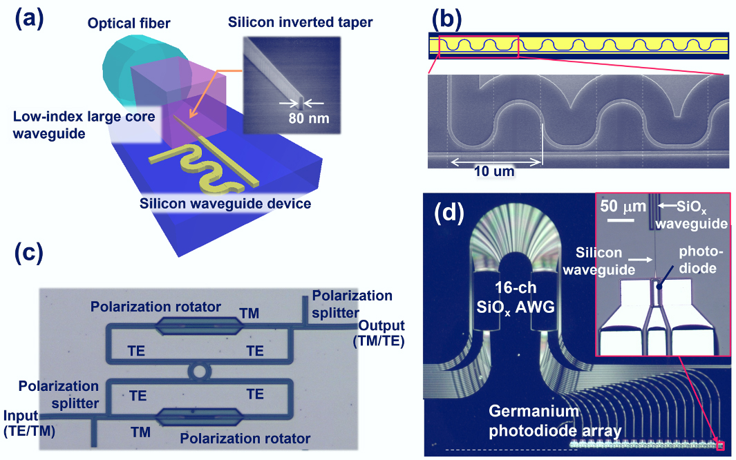
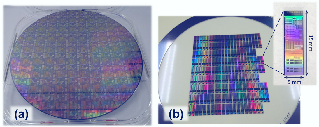
After the above-mentioned fundamental work, they extended their research to the development of monolithic photonic integration based on silicon-based photonic wiring elements, silicon optical modulators, germanium photodetectors and high-performance passive devices using medium index materials. They also became among the first to demonstrate the integration of high-speed electronics circuits on a silicon photonic platform by using surface-mounted hybrid integration technology. Figure 2(d) shows an example of a monolithic photonic integration, which includes a high-performance AWG filter and germanium photodiodes. These integration technologies enable high-performance photonic-electronic integrated circuits and are now widely used both in R&D and commercial foundries. Then they carried this forward in the development of silicon photonics technology based on standard CMOS fabrication processes in AIST. In the institute, they have established a public silicon photonics foundry service utilizing 300-mm wafer CMOS processes with an ultra-fine ArF immersion lithography [7]. Typical products of the service are shown in Fig. 3. Moreover, they have been making a significant efforts for the construction of an R&D ecosystem, which supports the development of supply-chain technologies.
These achievements of the recipients are significant both for the progress of the technology and for the industrial implementation of silicon integrated photonic circuits, enough to make them worthy of the Society’s Achievement Award.
References
- T. Shoji, T. Tsuchizawa, T. Watanabe, K. Yamada, H. Morita, “Low loss mode size converter from 0.3-μm square Si wire waveguides to singlemode fibres,” Electronics Letters, vol. 38, pp.1669-1670 (2002)
- T. Tsuchizawa, K. Yamada, H. Fukuda, T. Watanabe, J. Takahashi, M. Takahashi, T. Shoji, E. Tamechika, S. Itabashi, and H. Morita, “Microphotonics Devices Based on Silicon Micro-Fabrication Technology,” IEEE Journal Selected Topics in Quantum Electronics, vol. 11, pp.232-240 (2005)
- K. Yamada, T. Shoji, T. Tsuchizawa, T. Watanabe, J. Takahashi, S. Itabashi, “Silicon-wire-based ultrasmall lattice filters with wide free spectral ranges,” Optics Letters vol. 28, pp.1663-1664 (2003)
- H. Fukuda, K. Yamada, T. Tsuchizawa, T. Watanabe, H. Shinojima and S. Itabashi, “Silicon photonic circuits with polarization diversity,” Optics Express, Vol.16, pp.4872-4880 (2008)
- H. Fukuda, K. Yamada, T. Shoji, M. Takahashi, T. Tsuchizawa, T. Watanabe, J. Takahashi, and S. Itabashi, “Four-wave mixing in silicon wire waveguides,” Optics Express, Vol. 13, pp.4629-4637 (2005)
- K. Yamada, T. Tsuchizawa, H. Nishi, R. Kou, T. Hiraki, K. Takeda, H. Fukuda, Y. Ishikawa, K. Wada, and T. Yamamoto, “High-performance silicon photonics technology for telecommunications applications,” Science and technology of advanced materials 15 (2), 024603, (2014).
- https://www.aist.go.jp/aist_j/press_release/pr2020/pr20200227/pr20200227.html (in Japanese)