Achievement Award
Pioneering research on terahertz radiation sources and detectors based on two-dimensional plasmon resonance phenomena
Terahertz (THz) waves, which are situated in the electromagnetic spectrum between radio waves and light waves, are an untapped frequency resource that is essential for realizing Society 5.0. Potential applications of THz waves include imaging and identification of materials without risk from ionizing radiation exposure, as well as next-generation 6G and 7G ultrahigh-speed wireless communications. However, conventional THz devices have a substantial physical limitation called the “THz gap,” and overcoming this limitation has become one of the highest priorities.
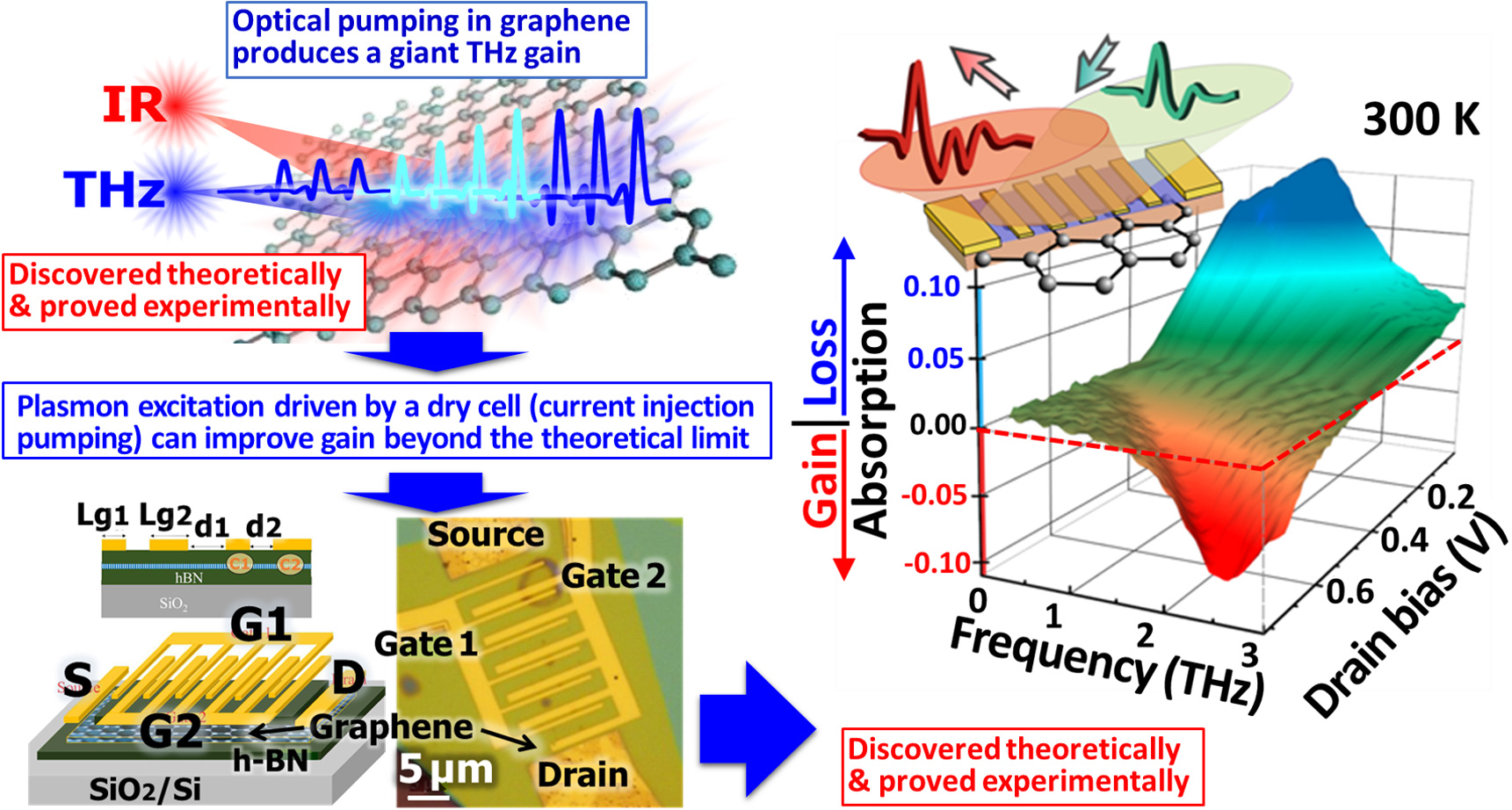
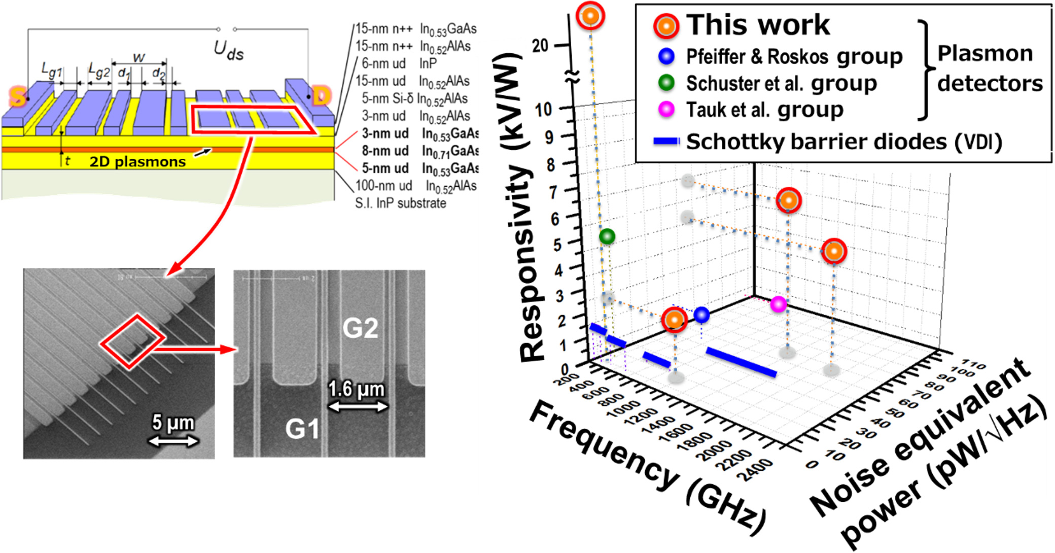
Through breakthroughs leading to the introduction of new materials, principles, and structures, the awardee, Professor Taiichi Otsuji, has developed high-intensity THz radiation sources and high-sensitive, fast-response THz detectors. Both the sources and detectors are fully integrated and operate at room temperature, allowing them to overcome the THz gap. First, using his original infrared laser two-photon wave mixing method, he demonstrated for the first time that two-dimensional plasmons, which are quanta of the collective oscillation of charge density waves of two-dimensional electrons aggregated in a transistor channel, resonate in the THz band, even at room temperature [1]. This provided the first experimental validation of two-dimensional plasmon resonances at room temperature whose theory was originally discovered by M. Dyakonov and M. Shur [2]. Second, Professor Otsuji succeeded in both the theoretical discovery and experimental demonstration of light amplification by stimulated emission of THz radiation in optically pumped graphene [3,4] and the giant gain enhancement effect of graphene Dirac plasmons on THz stimulated emissions [5] (Fig. 1). Based on these results, he designed and fabricated prototype graphene laser transistor devices with a unique distributed-feedback dual-gate structure, and experimentally demonstrated single-mode coherent THz emission and broadband amplified spontaneous THz emission by current-injection pumping at 100 K [6]. These breakthroughs have paved the way for the application of graphene in THz lasers. Third, he devised a new device structure called an asymmetric dual-grating gate (ADGG), which is effective for promoting highly efficient THz rectification and plasmon instabilities. Then, he fabricated a prototype transistor device using InP-based heterostructure quantum wells. This device increased the sensitivity by more than an order of magnitude compared to what was previously recorded by Schottky barrier diodes, and with better low-noise performance [7] (Figure 2). The superior performance of the ADGG detector device has been confirmed for high-speed THz wireless communications and for contactless, nondestructive imaging in safety and security applications [8].
For these pioneering achievements, Professor Otsuji was honored with the Commendation for Science and Technology by the Minister of Education, Culture, Sports, Science and Technology, and with many other awards from related prominent academic societies and international conferences. Fourth, he applied the aforementioned ADGG structure to graphene transistors and, in a world first, successfully demonstrated that the application of a DC voltage alone can excite graphene plasmon instabilities, resulting in THz gain amplification that exceeds the theoretical limit on direct interaction between graphene electrons and THz photons by a factor of four, even at room temperature [9, 10] (Figure 1). This is a pioneering achievement that will contribute to the realization of room-temperature, high-intensity THz lasers, and represents a breakthrough for improving the lasing threshold temperature and ultra-high gain of graphene THz lasers. This will also open up new horizons in light source and detection device technologies for next-generation 6G and 7G ultrafast wireless communications.
As described above, the awardee's achievements are remarkable and well deserving of the Society's Achievement Award.
References
- T. Otsuji, M. Hanabe and O. Ogawara, “Terahertz plasma wave resonance of two-dimensional electrons in InGaP/InGaAs/GaAs high-electron-mobility transistors,” Applied Physics Letters, vol. 85, no. 11, pp. 2119-2121, 2004.
- M. Dyakonov, and M. Shur, “Shallow water analogy for a ballistic field effect transistor: New mechanism of plasma wave generation by dc current,” Physical Review Letters, vol. 71, iss. 15, pp. 2465-2468, 1993.
- V. Ryzhii, M. Ryzhii, and T. Otsuji, “Negative dynamic conductivity of graphene with optical pumping,” Journal of Applied Physics, vol. 101, no. 7, pp. 083114-1-4, 2007.
- T. Otsuji, S. A. Boubanga Tombet, A. Satou, H. Fukidome, M. Suemitsu, E. Sano, V. Popov, M. Ryzhii, and V. Ryzhii, “Graphene-based devices in terahertz science and technology,” Journal of Physics D: Applied Physics, vol. 45, no. 30, pp. 303001-1-9, 2012. (invited)
- T. Watanabe, T. Fukushima, Y. Yabe, S.A. Boubanga Tombet, A. Satou, A.A. Dubinov, V. Ya Aleshkin, V. Mitin, V. Ryzhii, and T. Otsuji, “The gain enhancement effect of surface plasmon polaritons on terahertz stimulated emission in optically pumped monolayer graphene,” New Journal of Physics, vol. 15, iss. 7, pp. 075003-1-11, 2013.
- D. Yadav, G. Tamamushi, T. Watanabe, J. Mitsushio, Y. Tobah, K. Sugawara, A.A. Dubinov, A. Satou, M. Ryzhii, V. Ryzhii, and T. Otsuji, “Terahertz light-emitting graphene-channel transistor toward single-mode lasing,” Nanophotonics, vol. 7, iss. 4, pp. 741-752, 2018.
- T. Otsuji, T. Watanabe, S. Boubanga Tombet, A. Satou, W. Knap, V. Popov, M. Ryzhii, and V. Ryzhii, “Emission and detection of terahertz radiation using two-dimensional electrons in III-V semiconductors and graphene,” IEEE Transactions on Terahertz Science and Technology, vol. 3, no. 1, pp. 63-71, 2013.
- W. Knap, M. Dyakonov, D. Coquillat, F. Teppe, N. Dyakonova, J. Lusakowski, K. Karpierz, M. Sakowicz, G. Valusis, D. Seliuta, I. Kasalynas, A. El Fatimy, Y. M. Meziani, and T. Otsuji, “Field effect transistors for terahertz detection: physics and first imaging applications,” Journal of Infrared, Millimeter, and Terahertz Waves, vol. 30, no. 12, pp. 1319-1337, 2009.
- S. Boubanga-Tombet, W. Knap, D. Yadav, A. Satou, D.B. But, V.V. Popov, I.V. Gorbenko, V. Kachorovskii, and T. Otsuji, “Room temperature amplification of terahertz radiation by grating-gate graphene structures,” Physical Review X, vol. 10, iss. 3, pp. 031004-1-19, 2020.
- Stephane Albon Boubanga-Tombet, Akira Satou, Deepika Yadav, Dmitro B But, Wojciech Knap, Vyacheslav V Popov, Iliya V Gorbenko, Valentin Kachorovskii and Taiichi Otsuji, “Paving the way for tunable graphene plasmonic THz amplifiers,” Frontiers in Physics, vol. 9, pp. 726806-1-10, 2021. (invited, review)