Achievement Award
Integrated Circuit Design Education and Research at the VLSI Design and Education Center (VDEC)
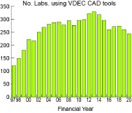
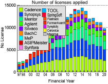
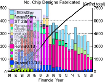
Since the VLSI Design and Education Center (VDEC) was established at the University of Tokyo in 1996 and shared by users all over Japan, it has made a great contribution to the design education and research of integrated circuits at Japanese universities. In integrated circuit design in Japan before the opening of the VDEC, individual researchers had to procure EDA (Electronic Design Automation) tools necessary for the design and contract of trial production and the monetary and human costs were enormous, and as a result, few university researchers were involved in integrated circuit design research. The VDEC made a one-time contract for EDA tools, supplied licenses to technical colleges and universities, and provided a shuttle service that aggregates design data and makes prototypes at low cost. This greatly reduced the burden on faculty members and students and played a major role in expanding the base of the academic field in Japan. The number of EDA tool licenses was about 2,000 when it was first opened, but exceeded 10,000 in 2005. The number of prototype chips was less than 100 in the year of establishment but exceeded 500 in 2006. Before the opening of the VDEC, that number was less than 10 per year.
Processes that can be prototyped continue to change with the miniaturization of process rules, 0.6 μm, 0.5 μm, 0.35 μm, 0.18 μm, 0.15 μm, 90 nm, 65 nm, 45 nm, and 28 nm in addition to the very inexpensive 1.2 / 0.8 μm process that has continued since its inception. Over the 24 years since the inauguration of the VDEC, more than 8,100 varieties have been prototyped. CAD training, which is a training course on how to use EDA tools, was started in 1997, and hands-on tutorial-like education for working adults and students was started in 1998, and both have been held while continuing to be updated until now.
Furthermore, in 1997, the "Young People's Association for Supporting the VDEC" was held as a place for the exchange of information between young researchers and students. In 1998, the name was changed to "Designer's Forum", and more than 1,000 people participated in the 24 meetings. In addition to exchanging information, commendations for circuits designed by students are also provided, which leads to motivation for students to research. As a result, the number of papers published related to VDEC activities has exceeded 16,000 in the past 24 years.
The award recipients have made great efforts to develop human resources through integrated circuit design education and research activities at the VDEC. Award recipient Asada created the basic activity policy and served as the director of the VDEC for 18 years from 2000 to 2018 when he retired, making a great contribution to its operation. Award recipient Ikeda was hired as an assistant at the same time as the establishment of VDEC, and after working as an associate professor, he has been a professor since 2013 and has been deeply involved in whole work of the VDEC. In addition, the VDEC has restarted as a division due to the reorganization accompanying the establishment of the University of Tokyo System Design Research Center (d.lab) in 2019. After the reorganization, Award recipient Ikeda continues to coordinate the two major projects of the former VDEC, which is the supply of EDA licenses and the compilation of prototype data, as the head of the basic design research division of d.lab. As mentioned above, the award recipients’ contributions to the VDEC for more than 20 years have been indispensable to the development of the integrated circuit field in Japan, and their devoted activities are considered to be an extremely large achievement that corresponds to the achievement award.
References
- K. Asada, “アナログ電子回路―VLSI工学へのアプローチ”, Shoukoudou, Tokyo, 1998.
- K. Asada, M. Ikeda et al., “ディジタル集積回路の設計と試作”, Baifukan, Tokyo, 1998.
- K. Asada et al., “システムLSI設計自動化技術の基礎―パブリックドメインツールの利用法”, Baifukan, Tokyo, 2005.
- K. Asada et al., “アナログRF CMOS集積回路設計 基礎編/応用編”, Baifukan, Tokyo, 2010/2011.
- K. Asada et al., “はかる×わかる半導体 入門編”, Nikkei BP Consulting, Tokyo, 2013.
- K. Asada, “集積回路設計”, Corona Publishing Co., LTD., Tokyo, 2015.
- K. Asada et al. “はかる×わかる半導体 応用編”, Nikkei BP Consulting, Tokyo, 2019
- M. Ikeda, “MOSによる電子回路基礎”, Suurikougaku-sha, Tokyo, 2011
- M. Ikeada, “NANO-CHIPS 2030”, Springer, Germany, 2020.